
FemtoClock NG Universal Frequency Translator
NOTICE - The following device(s) are recommended alternatives:
Jump to Page Section:
Overview
Description
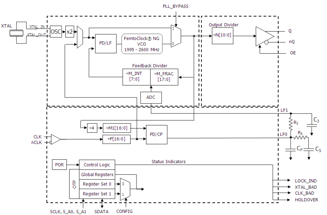
The IDT8T49N105I is a highly flexible FemtoClock® NG general purpose, low phase noise Universal Frequency Translator / Synthesizer with alarm and monitoring functions suitable for networking and communications applications. It is able to generate any output frequency in the 0.98MHz - 312.5MHz range and most output frequencies in the 312.5MHz - 1,300MHz range.
The IDT8T49N105I has three operating modes to support a very broad spectrum of applications:Frequency Synthesizer, High-Bandwidth Frequency Translator or Low-Bandwidth Frequency Translator. This device provides two factory-programmed default power-up configurations burned into One-Time Programmable (OTP) memory. The configuration to be used is selected by the CONFIG pin. The two configurations are specified by the customer and are programmed by IDT during the final test phase from an on-hand stock of blank devices. The two configurations may be completely independent of one another. To implement other configurations, these power-up default settings can be overwritten after power-up using the I2C interface and the device can be completely reconfigured. However, these settings would have to be re-written next time the device powers-up.
To see other devices in this product family, visit the Universal Frequency Translators page.
Features
-
Fourth generation FemtoClock® NG technology
-
Universal Frequency Translator (UFT) / Frequency Synthesizer
-
Single output (Q, nQ), programmable as LVPECL or LVDS
-
Zero ppm frequency translation
-
Single differential input supports the following input types: LVPECL, LVDS, LVHSTL, HCSL
-
Input frequency range: 8kHz - 710MHz
-
Crystal input frequency range: 16MHz - 40MHz
-
Two factory-set register configurations for power-up default state
-
Power-up default configuration pin or register selectable
-
Configurations customized via One-Time Programmable ROM
-
Settings may be overwritten after power-up via I2C
-
I2C Serial interface for register programming
-
RMS phase jitter at 155.52MHz, using a 40MHz crystal LVDS Output (12kHz - 20MHz): 439fs (typical), Low Bandwidth Mode (FracN)
-
RMS phase jitter at 400MHz, using a 40MHz crystal (12kHz - 40MHz):285fs (typical), Synthesizer Mode (Integer FB)
- Output supply voltage modes:
- VCC/VCCA/VCCO
- 3.3V/3.3V/3.3V
- 3.3V/3.3V/2.5V (LVPECL only)
- 2.5V/2.5V/2.5V
- -40°C to 85°C ambient operating temperature
- Lead-free (RoHS 6) packaging
Comparison
Applications
Design & Development
Models
ECAD Models
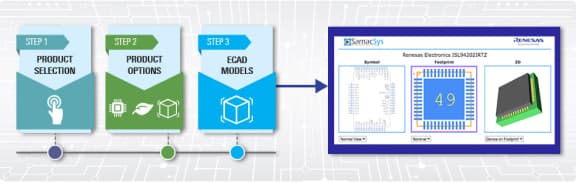
Schematic symbols, PCB footprints, and 3D CAD models from SamacSys can be found by clicking on products in the Product Options table. If a symbol or model isn't available, it can be requested directly from the website.
Processing table
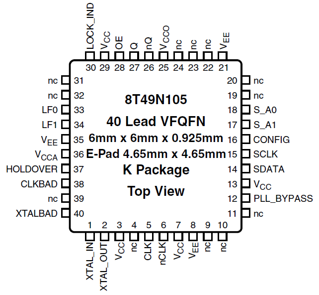
| VFQFPN | 40 | I | Yes | Tray | ||
| VFQFPN | 40 | I | Yes | Reel | ||
| VFQFPN | 40 | I | Yes | Tray | ||
| VFQFPN | 40 | I | Yes | Reel |
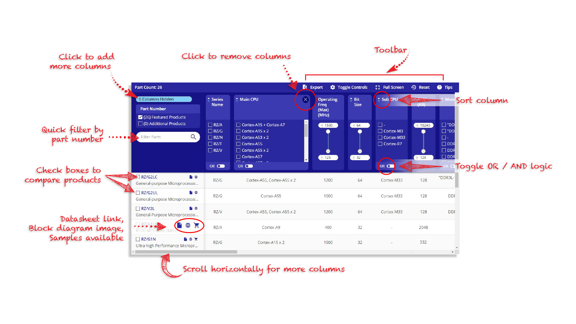
Tips for Using This Parametric Table:
- Hide Filters button in header: Collapse or expands filters
- Column sort buttons in header: Sort Column alphabetically / numerically descending or ascending
- Reset button in header: Reset all filters to the page default
- Full Screen button in header: Expand the table to full screen view (user must close out of full screen before they can interact with rest of page)
- Export button in header: Export the filtered results of the table to an Excel document
- Filter parts search bar in header: Type to filter table results by part number
- Hide column button in column headers: Select to hide columns in table
- AND / OR toggle switches in header: Toggles the logic of this particular filter to be “AND” or “OR” logic for filtering results
- Multiselect checkboxes at beginning of each row in table: Select these checkboxes to compare products against each other
- Document icon next to product name in row: View the featured document for this product
- Chip icon next to the right of the document icon in row: View the block diagram for this product
- Cart icon to the right of the chip icon: Indicates that samples are available for this product