
FemtoClock® Crystal-to-LVDS 8-Output Clock Synthesizer
Jump to Page Section:
Overview
Description
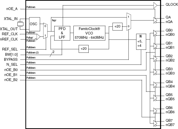
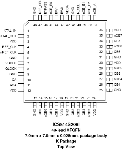
The 814S208I is an eight LVDS output clock synthesizer designed for wireless infrastructure applications. The device generates eight copies of a selectable 122.88MHz or 153.6MHz clock signal with excellent phase jitter performance. The PLL is optimized for a reference frequency of 30.72MHz. Both a crystal interface and a differential system clock input are supported for the reference frequency. An extra LVDS output duplicates the reference frequency and is provided for clock tree cascading. The device uses IDT's third generation FemtoClock® technology for an optimum of high clock frequency and low phase noise performance, combined with a low power consumption. A PLL lock status output is provided for monitoring and diagnosis purpose. The device supports a 3.3V voltage supply and is packaged in a small, lead-free (RoHS 6) 48-lead VFQFN package. The extended temperature range supports wireless infrastructure, telecommunication and networking end equipment requirements.
Features
- Third generation FemtoClock® technology
- Selectable 122.88MHz or 153.6MHz output clock synthesized from a 30.72MHz fundamental mode crystal
- Eight differential LVDS clock outputs
- Differential reference clock input pair
- PLL lock indicator output
- Crystal interface designed for a 30.72MHz, parallel resonant crystal
- RMS phase jitter @ 122.88MHz, using a 30.72MHz crystal (12kHz - 20MHz): 0.650ps (typical)
- RMS phase jitter @ 153.6MHz, using a 30.72MHz crystal (12kHz - 20MHz): 0.642ps (typical)
- LVCMOS interface levels for the control input
- Full 3.3V supply voltage
- Available in Lead-free (RoHS 6) 48-lead VFQFN package
- -40°C to 85°C ambient operating temperature
Comparison
Applications
Design & Development
Models
ECAD Models
Schematic symbols, PCB footprints, and 3D CAD models from SamacSys can be found by clicking on products in the Product Options table. If a symbol or model isn't available, it can be requested directly from the website.
Processing table
| VFQFPN | 48 | I | Yes | Tray | ||
| VFQFPN | 48 | I | Yes | Reel |
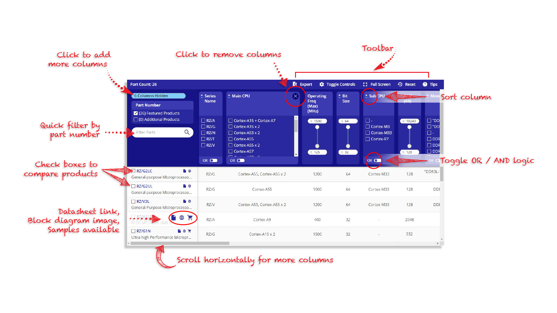
Tips for Using This Parametric Table:
- Hide Filters button in header: Collapse or expands filters
- Column sort buttons in header: Sort Column alphabetically / numerically descending or ascending
- Reset button in header: Reset all filters to the page default
- Full Screen button in header: Expand the table to full screen view (user must close out of full screen before they can interact with rest of page)
- Export button in header: Export the filtered results of the table to an Excel document
- Filter parts search bar in header: Type to filter table results by part number
- Hide column button in column headers: Select to hide columns in table
- AND / OR toggle switches in header: Toggles the logic of this particular filter to be “AND” or “OR” logic for filtering results
- Multiselect checkboxes at beginning of each row in table: Select these checkboxes to compare products against each other
- Document icon next to product name in row: View the featured document for this product
- Chip icon next to the right of the document icon in row: View the block diagram for this product
- Cart icon to the right of the chip icon: Indicates that samples are available for this product