
1-to-5 Differential-to-3.3V LVPECL PLL Clock Driver W/Dynamic Clock Switch
Jump to Page Section:
Overview
Description
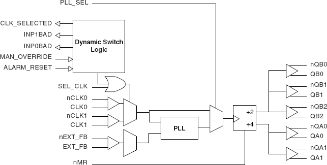
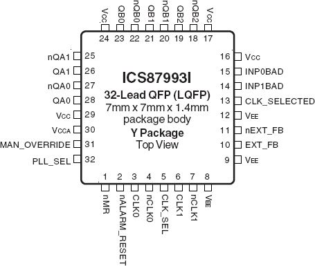
The 87993I is a PLL clock driver designed specifically for redundant clock tree designs. The device receives two differential LVPECL clock signals from which it generates 5 new differential LVPECL clock outputs. Two of the output pairs regenerate the input signal frequency and phase while the other three pairs generate 2x, phase aligned clock outputs. External PLL feedback is used to also provide zero delay buffer performance. The 87993I Dynamic Clock Switch (DCS) circuit continuously monitors both input CLK signals. Upon detection of a failure (CLK stuck HIGH or LOW for at least 1 period), the INP_BAD for that CLK will be latched (H). If that CLK is the primary clock, the DCS will switch to the good secondary clock and phase/frequency alignment will occur with minimal output phase disturbance. The typical phase bump caused by a failed clock is eliminated.
Features
- 5 differential 3.3V LVPECL outputs
- Selectable differential clock inputs
- CLKx, nCLKx pair can accept the following differential input levels: LVPECL, LVDS, LVHSTL, HCSL, SSTL
- Output frequency range: 50MHz to 250MHz
- VCO range: 200MHz to 500MHz
- External feedback for "zero delay" clock regeneration with configurable frequencies
- Cycle-to-cycle jitter (RMS): 20ps (maximum)
- Output skew: 70ps (maximum), within one bank
- 3.3V supply voltage
- -40°C to 85°C ambient operating temperature
- Lead-Free package available
Comparison
Applications
Design & Development
Models
ECAD Models
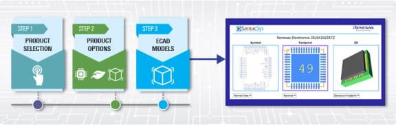
Schematic symbols, PCB footprints, and 3D CAD models from SamacSys can be found by clicking on products in the Product Options table. If a symbol or model isn't available, it can be requested directly from the website.
Processing table
| TQFP | 32 | I | Yes | Tray | ||
| TQFP | 32 | I | Yes | Reel |
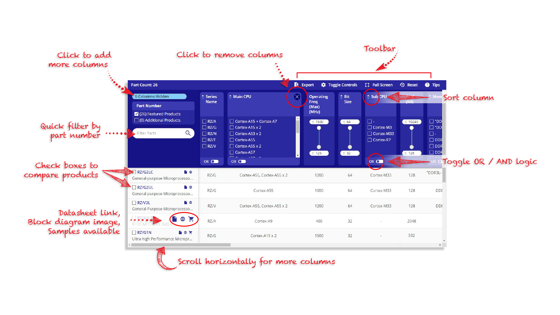
Tips for Using This Parametric Table:
- Hide Filters button in header: Collapse or expands filters
- Column sort buttons in header: Sort Column alphabetically / numerically descending or ascending
- Reset button in header: Reset all filters to the page default
- Full Screen button in header: Expand the table to full screen view (user must close out of full screen before they can interact with rest of page)
- Export button in header: Export the filtered results of the table to an Excel document
- Filter parts search bar in header: Type to filter table results by part number
- Hide column button in column headers: Select to hide columns in table
- AND / OR toggle switches in header: Toggles the logic of this particular filter to be “AND” or “OR” logic for filtering results
- Multiselect checkboxes at beginning of each row in table: Select these checkboxes to compare products against each other
- Document icon next to product name in row: View the featured document for this product
- Chip icon next to the right of the document icon in row: View the block diagram for this product
- Cart icon to the right of the chip icon: Indicates that samples are available for this product