
Low Voltage, Low Skew 3.3V LVPECL Clock Generator
Jump to Page Section:
Overview
Description
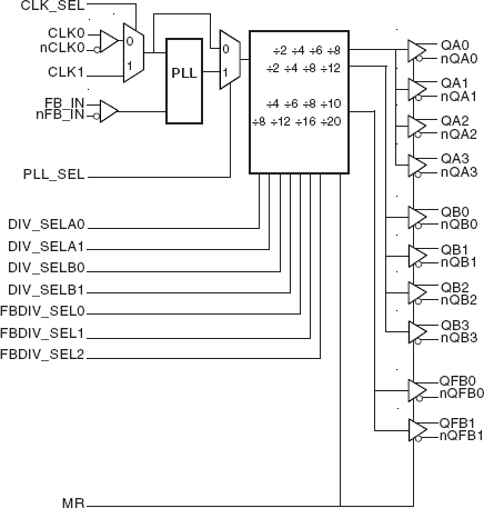
The 8732-01 is a low voltage, low skew, 3.3V LVPECL Clock Generator. The 8732-01 has two selectable clock inputs. The CLK0, nCLK0 pair can accept most standard differential input levels. The single ended clock input accepts LVCMOS or LVTTL input levels. The 8732-01 has a fully integrated PLL along with frequency configurable outputs. An external feedbackinput and outputs regenerate clocks with "zero delay". The 8732-01 has multiple divide select pins for each bank of outputs along with 3 independent feedback divide select pins allowing the 8732-01 to function both as a frequency multiplier and divider. The PLL_SEL input can be usedto bypass the PLL for test and system debug purposes.In bypass mode, the input clock is routed around the PLLand into the internal output dividers.
Features
- Ten differential 3.3V LVPECL outputs
- Selectable differential CLK0, nCLK0 or LVCMOS/LVTTL CLK1 inputs
- CLK0, nCLK0 supports the following input types: LVPECL, LVDS, LVHSTL, SSTL, HCSL
- CLK1 accepts the following input levels: LVCMOS or LVTTL
- Maximum output frequency: 350MHz
- VCO range: 250MHz to 700MHz
- External feedback for "zero delay" clock regeneration with configurable frequencies
- Cycle-to-cycle jitter: CLK0, nCLK0, 50ps (maximum) CLK1, 80ps (maximum)
- Output skew: 150ps (maximum)
- Static phase offset: -150ps to 150ps
- Lead-Free package fully RoHS compliant
Comparison
Applications
Design & Development
Models
ECAD Models
Schematic symbols, PCB footprints, and 3D CAD models from SamacSys can be found by clicking on products in the Product Options table. If a symbol or model isn't available, it can be requested directly from the website.
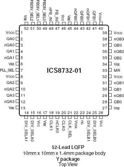
Processing table
| TQFP | 52 | C | Yes | Tray | ||
| TQFP | 52 | C | Yes | Reel |
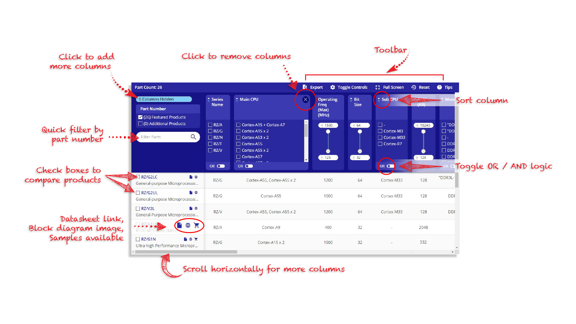
Tips for Using This Parametric Table:
- Hide Filters button in header: Collapse or expands filters
- Column sort buttons in header: Sort Column alphabetically / numerically descending or ascending
- Reset button in header: Reset all filters to the page default
- Full Screen button in header: Expand the table to full screen view (user must close out of full screen before they can interact with rest of page)
- Export button in header: Export the filtered results of the table to an Excel document
- Filter parts search bar in header: Type to filter table results by part number
- Hide column button in column headers: Select to hide columns in table
- AND / OR toggle switches in header: Toggles the logic of this particular filter to be “AND” or “OR” logic for filtering results
- Multiselect checkboxes at beginning of each row in table: Select these checkboxes to compare products against each other
- Document icon next to product name in row: View the featured document for this product
- Chip icon next to the right of the document icon in row: View the block diagram for this product
- Cart icon to the right of the chip icon: Indicates that samples are available for this product