
LVCMOS Zero Delay Buffer
NOTICE - The following device(s) are recommended alternatives:
Jump to Page Section:
Overview
Description
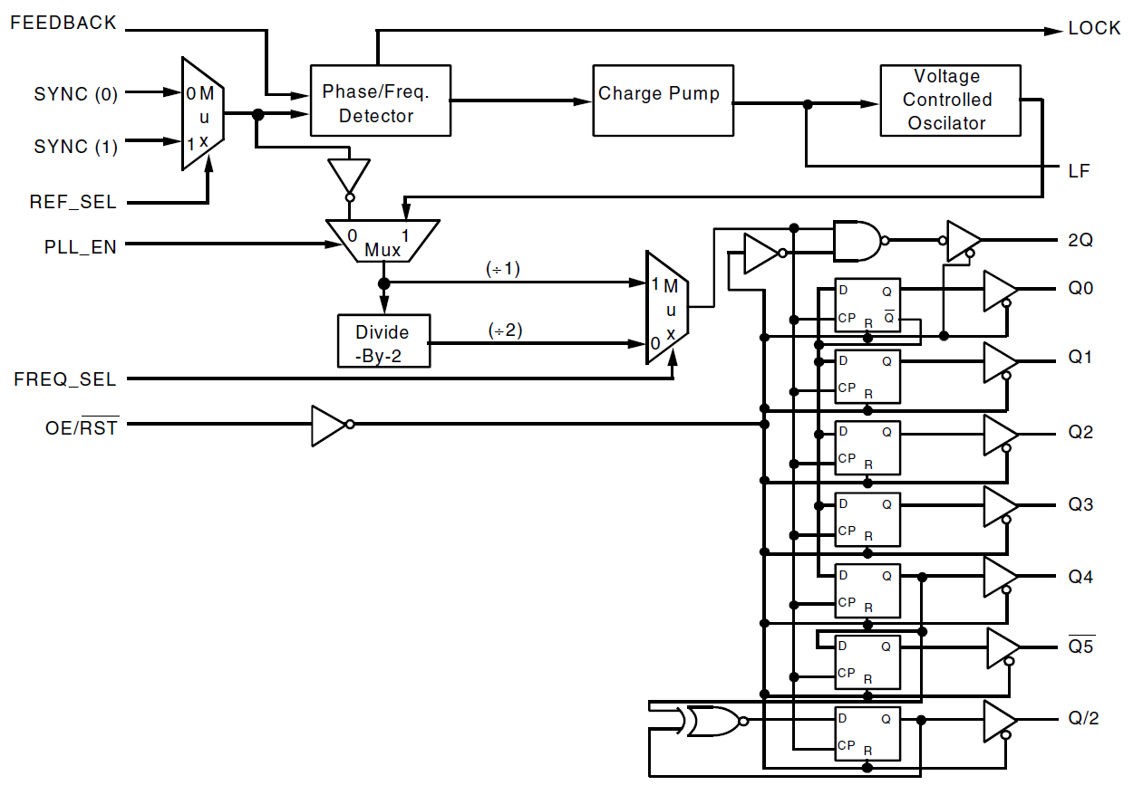
The FCT388915T uses phase-lock loop technology to lock the frequency and phase of outputs to the input reference clock. It provides low skew clock distribution for high performance PCs and workstations. One of the outputs is fed back to the PLL at the FEEDBACK input resulting in essentially zero delay across the device. The PLL consists of the phase/ frequency detector, charge pump, loop filter and VCO. The VCO is designed for a 2Q operating frequency range of 40MHz to f2Q Max. The FCT388915T provides 8 outputs, the Q5 output is inverted from the Q outputs. The 2Q runs at twice the Q frequency and Q/2 runs at half the Q frequency. The FREQ_SEL control provides an additional ÷ 2 option in the output path. PLL _EN allows bypassing of the PLL, which is useful in static test modes. When PLL_EN is low, SYNC input may be used as a test clock. In this test mode, the input frequency is not limited to the specified range and the polarity of outputs is complementary to that in normal operation (PLL_EN = 1). The LOCK output attains logic HIGH when the PLL is in steady-state phase and frequency lock. When OE/RST is low, all the outputs are put in high impedance state and registers at Q, Q and Q/2 outputs are reset. The FCT388915T requires one external loop filter component as recommended in Figure 3.
Features
- 0.5 MICRON CMOS Technology
- Input frequency range: 10MHz – f2Q Max. spec
- (FREQ_SEL = HIGH)
- Max. output frequency: 150MHz
- Pin and function compatible with FCT88915T, MC88915T
- 5 non-inverting outputs, one inverting output, one 2x output,
- one ÷2 output
- all outputs are TTL-compatible
- 3-State outputs
- Duty cycle distortion < 500ps (max.)
- 32/–16mA drive at CMOS output voltage levels
- VCC = 3.3V ± 0.3V
- Inputs can be driven by 3.3V or 5V components
- Available in 28 pin PLCC and SSOP packages
Comparison
Applications
Design & Development
Models
ECAD Models
Schematic symbols, PCB footprints, and 3D CAD models from SamacSys can be found by clicking on products in the Product Options table. If a symbol or model isn't available, it can be requested directly from the website.
Processing table
Pkg. Type |
Lead Count (#) |
Temp. Grade |
Pb (Lead) Free |
Carrier Type |
Buy / Sample |
|
|---|---|---|---|---|---|---|
| Part Number | ||||||
| PLCC | 28 | C | Yes | Tube | ||
| SSOP | 28 | C | Yes | Tube | ||
| SSOP | 28 | C | Yes | Reel | ||
| PLCC | 28 | C | Yes | Tube | ||
| PLCC | 28 | C | Yes | Reel | ||
| SSOP | 28 | C | Yes | Tube | ||
| SSOP | 28 | C | Yes | Reel | ||
| PLCC | 28 | C | Yes | Tube | ||
| PLCC | 28 | C | Yes | Reel | ||
| SSOP | 28 | C | Yes | Tube | ||
| SSOP | 28 | C | Yes | Reel | ||
| PLCC | 28 | C | Yes | Tube | ||
| PLCC | 28 | C | Yes | Reel | ||
| SSOP | 28 | C | Yes | Tube |
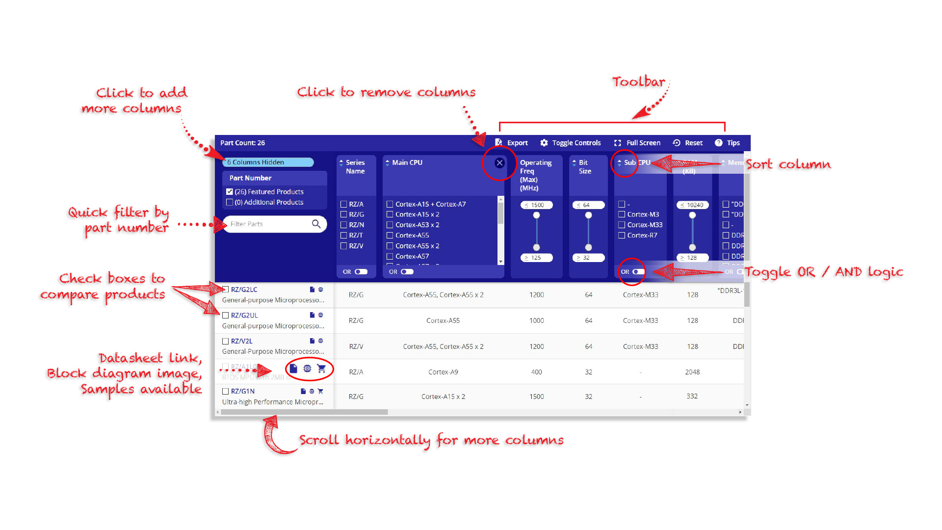
Tips for Using This Parametric Table:
- Hide Filters button in header: Collapse or expands filters
- Column sort buttons in header: Sort Column alphabetically / numerically descending or ascending
- Reset button in header: Reset all filters to the page default
- Full Screen button in header: Expand the table to full screen view (user must close out of full screen before they can interact with rest of page)
- Export button in header: Export the filtered results of the table to an Excel document
- Filter parts search bar in header: Type to filter table results by part number
- Hide column button in column headers: Select to hide columns in table
- AND / OR toggle switches in header: Toggles the logic of this particular filter to be “AND” or “OR” logic for filtering results
- Multiselect checkboxes at beginning of each row in table: Select these checkboxes to compare products against each other
- Document icon next to product name in row: View the featured document for this product
- Chip icon next to the right of the document icon in row: View the block diagram for this product
- Cart icon to the right of the chip icon: Indicates that samples are available for this product