
Differential-to-LVCMOS/LVTTL Fanout Buffer W/Divider And Glitchless Switch
Jump to Page Section:
Overview
Description
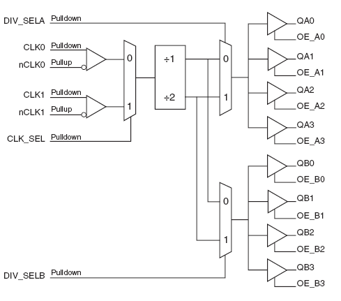
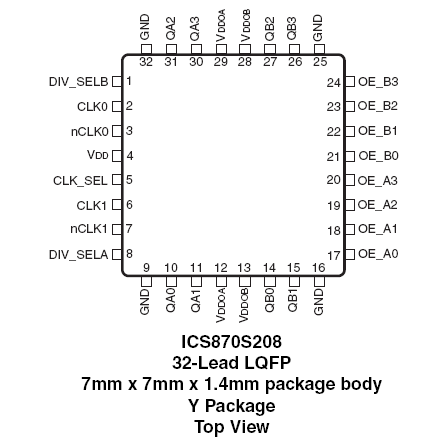
The 870S208 is a low skew, 8 output LVCMOS / LVTTL Fanout Buffer with selectable divider. The 870S208 has 2 selectable inputs that accept a variety of differential input types. The device provides the capability to suppress any glitch at the outputs of the device during an input clock switch to enhance clock redundancy in fault tolerant applications. The low impedance LVCMOS outputs are designed to drive 50? series or parallel terminated transmission lines. The effective fanout can be increased from 8 to 16 by utilizing the ability of the outputs to drive two series terminated lines. The divide select inputs, DIV_SELA and DIV_SELB, control the output frequency of each bank. The output banks can be independently selected for ÷1 or ÷2 operation. The output enable pins assigned to each output, support enabling and disabling of each output individually. The 870S208 is characterized at full 3.3V and 2.5V, and mixed 3.3V/2.5V output operating supply modes. Guaranteed output and part-to-part skew characteristics make the 870S208 ideal for high performance, single ended applications.
Features
- Eight LVCMOS/LVTTL outputs, (2 banks of 4 outputs) Each output has individual synchronous output enable
- Two selectable differential CLKx, nCLKx inputs
- Dual differential input pairs can accept the following differential input levels: LVPECL, LVDS, LVHSTL, SSTL, HCSL
- Maximum output frequency: 250MHz
- Selectable ÷1 or ÷2 operation
- Glitchless output behavior during input switch
- Output skew: 50ps (typical), 3.3V
- Bank skew: 30ps (typical), 3.3V
- Supply modes: Core/Output 3.3V/3.3V 2.5V/2.5V 3.3V/2.5V
- 0°C to 70°C ambient operating temperature
- Available in both standard (RoHS 5) and lead-free (RoHS 6) packages
Comparison
Applications
Design & Development
Models
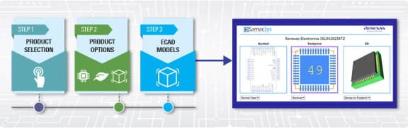
ECAD Models
Schematic symbols, PCB footprints, and 3D CAD models from SamacSys can be found by clicking on products in the Product Options table. If a symbol or model isn't available, it can be requested directly from the website.
Processing table
| VFQFPN | 32 | C | Yes | Tray |
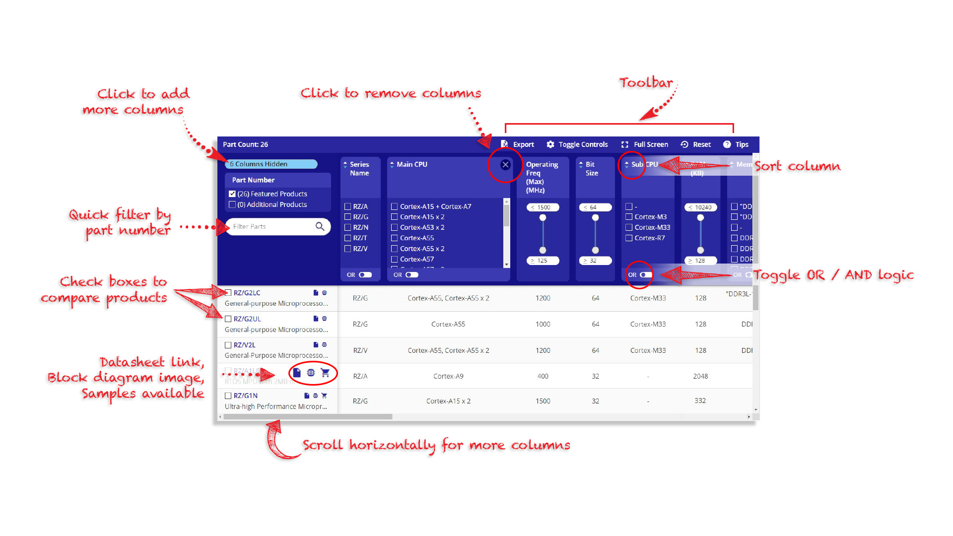
Tips for Using This Parametric Table:
- Hide Filters button in header: Collapse or expands filters
- Column sort buttons in header: Sort Column alphabetically / numerically descending or ascending
- Reset button in header: Reset all filters to the page default
- Full Screen button in header: Expand the table to full screen view (user must close out of full screen before they can interact with rest of page)
- Export button in header: Export the filtered results of the table to an Excel document
- Filter parts search bar in header: Type to filter table results by part number
- Hide column button in column headers: Select to hide columns in table
- AND / OR toggle switches in header: Toggles the logic of this particular filter to be “AND” or “OR” logic for filtering results
- Multiselect checkboxes at beginning of each row in table: Select these checkboxes to compare products against each other
- Document icon next to product name in row: View the featured document for this product
- Chip icon next to the right of the document icon in row: View the block diagram for this product
- Cart icon to the right of the chip icon: Indicates that samples are available for this product