
Overview
Description
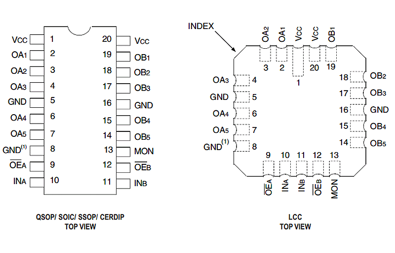
This buffer/clock driver is built using advanced dual metal CMOS technology. The FCT805T is a non-inverting clock driver consisting of two banks of drivers. Each bank drives five output buffers from a standard TTL compatible input. This part has extremely low output skew, pulse skew, and package skew. The device has a "heart-beat" monitor for diagnostics and PLL driving. The monitor output is identical to all other outputs and complies with the output specifications in this document. The FCT805T is designed for fast, clean edge rates to provide accurate clock distribution in high speed systems.

Features
- 0.5 MICRON CMOS Technology
- Guaranteed low skew < 500ps (max.)
- Very low duty cycle distortion < 600ps (max.)
- Low CMOS power levels
- TTL compatible inputs and outputs
- TTL level output voltage swings
- High drive: -32mA IOH, +48mA IOL
- Two independent output banks with 3-state control
- 1:5 fanout per bank
- "Heartbeat" monitor output
- ESD > 2000V per MIL-STD-883, Method 3015
- > 200V using machine model (C = 200pF, R = 0)
- Available in the following packages: – Commercial: QSOP, SOIC, SSOP – Military: CERDIP, LCC
Comparison
Applications
Design & Development
Models
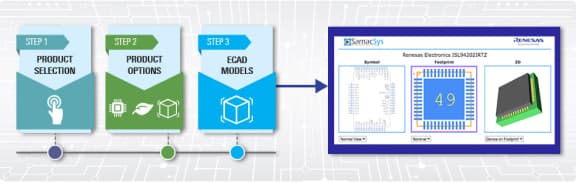
ECAD Models
Schematic symbols, PCB footprints, and 3D CAD models from SamacSys can be found by clicking on products in the Product Options table. If a symbol or model isn't available, it can be requested directly from the website.
Processing table
Pkg. Type |
Lead Count (#) |
Temp. Grade |
Pb (Lead) Free |
Carrier Type |
Buy / Sample |
|
|---|---|---|---|---|---|---|
| Part Number | ||||||
| CDIP | 20 | M | No | Tube | ||
| LCC | 20 | M | No | Tube | ||
| SSOP | 20 | C | No | Tube | ||
| SSOP | 20 | C | Yes | Tube | ||
| SSOP | 20 | C | Yes | Reel | ||
| QSOP | 20 | C | No | Tube | ||
| QSOP | 20 | C | Yes | Tube | ||
| QSOP | 20 | C | Yes | Reel | ||
| SOIC | 20 | C | Yes | Tube | ||
| SOIC | 20 | C | Yes | Reel | ||
| CDIP | 20 | M | No | Tube | ||
| LCC | 20 | M | No | Tube | ||
| SSOP | 20 | C | No | Tube | ||
| SSOP | 20 | C | Yes | Tube | ||
| SSOP | 20 | C | Yes | Reel | ||
| QSOP | 20 | C | No | Tube | ||
| QSOP | 20 | C | Yes | Tube | ||
| QSOP | 20 | C | Yes | Reel | ||
| SOIC | 20 | C | Yes | Tube | ||
| SOIC | 20 | C | Yes | Reel |
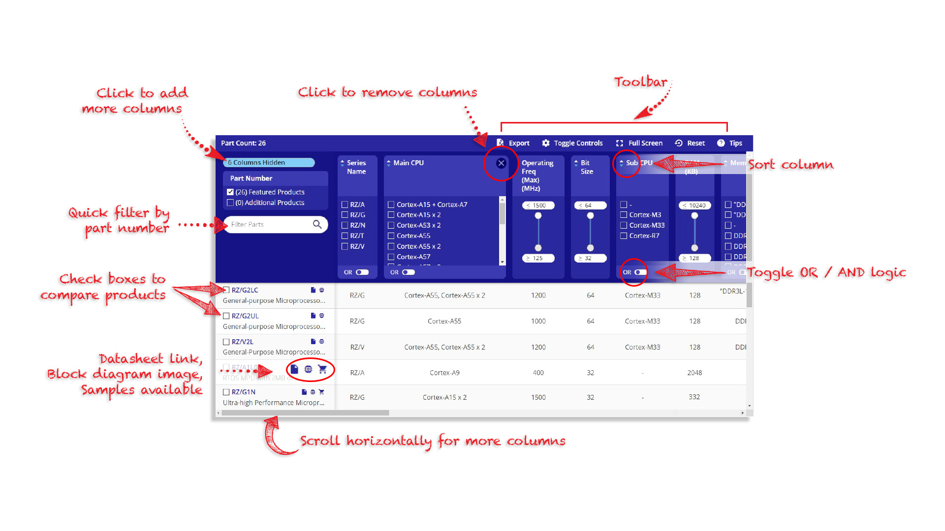
Tips for Using This Parametric Table:
- Hide Filters button in header: Collapse or expands filters
- Column sort buttons in header: Sort Column alphabetically / numerically descending or ascending
- Reset button in header: Reset all filters to the page default
- Full Screen button in header: Expand the table to full screen view (user must close out of full screen before they can interact with rest of page)
- Export button in header: Export the filtered results of the table to an Excel document
- Filter parts search bar in header: Type to filter table results by part number
- Hide column button in column headers: Select to hide columns in table
- AND / OR toggle switches in header: Toggles the logic of this particular filter to be “AND” or “OR” logic for filtering results
- Multiselect checkboxes at beginning of each row in table: Select these checkboxes to compare products against each other
- Document icon next to product name in row: View the featured document for this product
- Chip icon next to the right of the document icon in row: View the block diagram for this product
- Cart icon to the right of the chip icon: Indicates that samples are available for this product